

Keep up with the ever-evolving AI landscape
Unlock exclusive AI content by subscribing to our newsletter!!
The process removes glass bonding layers – and lowers defect rates.
As semiconductors continued to get smaller, chipmakers began to strain the limits of Moore’s Law, which postulates that the number of transistors on a microchip would double every two years to yield much faster computational power in smaller chips.
Now, IBM and Tokyo Electron (TEL) said they found a new method to save Moore’s Law and simplify the supply chain for chipmaking.
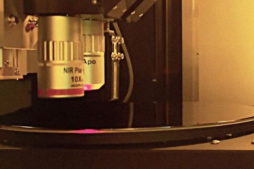
The two developed a new method for 3D chip stacking that can produce 300 millimeter silicon chip wafers, an apparent world’s first. IBM said chip stacking can potentially expand the number of transistors in a given volume – rather than an area, as Moore’s Law calls for.
IBM and TEL said they created the 300 millimeter module using an “infrared laser to enable a debonding process that’s transparent to silicon — meaning standard silicon wafers can be used” without needing a temporary glass layer for processing.
“As the global chip shortage continues, we’ll likely need novel ways to increase chip production capacity over the coming years,” IBM said in a blog. “We hope our work will help cut down on the number of products needed in the semiconductor supply chain, while also helping drive processing power improvements for years to come.”
The project is a culmination of four years of work. The pair plan further tests, which will examine ways to implement the process into a full semiconductor manufacturing flow.
To date, chip stacking is only seen in high-end operations such as the production of high-bandwidth memory. However, IBM and TEL believe it has the potential to expand the number of transistors in a specific volume.
Chip-stacking architectures require vertical connections between layers of silicon called through-silicon vias (TSVs). These are small connections that allow for a current to flow between one silicon layer to another, essentially letting each layer to 'talk' to the others.
The process involves thinning a silicon wafer to reveal the fabrication of TSVs required for vertical stacking.
To transport these thin, fragile silicon wafers, manufacturers introduce glass to the process to create a bonding layer so the wafers can be transported without damage. Once processed, the glass is removed via ultraviolet lasers.
IBM and TEL’s novel method removes the need for glass – and reportedly leads to fewer defects during production, which in turn would ease the growing strain placed on chipmakers.
The global chip shortage has seen production decrease due to factors such as the pandemic and ever-increasing demand. However, signs are emerging that the chip shortage may be easing, according to Omdia analyst Alexander Harrowell.
You May Also Like
.jpg?width=700&auto=webp&quality=80&disable=upscale)
.jpg?width=700&auto=webp&quality=80&disable=upscale)
.jpg?width=700&auto=webp&quality=80&disable=upscale)


.jpg?width=300&auto=webp&quality=80&disable=upscale)

.jpg?width=300&auto=webp&quality=80&disable=upscale)