Keep up with the ever-evolving AI landscape
Unlock exclusive AI content by subscribing to our newsletter!!
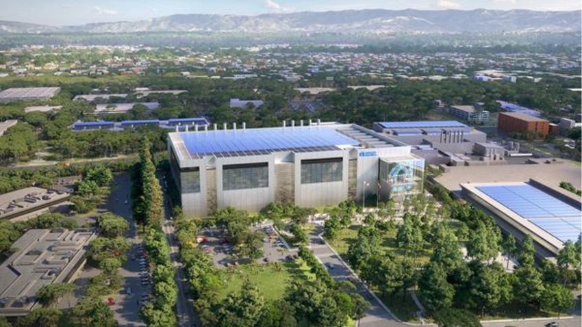
Chip equipment giant Applied Materials is investing up to $4 billion to build what it says will be a “unique” semiconductor research and development center the size of three football fields in the heart of Silicon Valley.
Called EPIC (Equipment and Process Innovation and Commercialization) Center, the facility will be the largest of its kind in the world at 180,000 square feet, according to the company. To open in early 2026, the center will be built near Applied Materials' headquarters in Santa Clara, California.
In a first, the center will bring together chipmakers, academic researchers and ecosystem partners in one central hub. The center is expected to hasten manufacturing innovation, lower costs and reduce − by several years − the time it takes for products to move from concept to commercialization.
In another first, chipmakers will have their own dedicated space within an equipment manufacturer facility to gain early access to the latest tools and technologies so they can accelerate development of their own products.
Potential partners for the center include AMD, Intel, IBM, Micron, Nvidia, Samsung, TSMC and Western Digital whose executives recorded videos to accompany the Applied Materials’ announcement.
This breadth and scale of capabilities under one roof makes the center “unique” in the industry, according to Applied Materials.
The company expects to further invest more than $25 billion in R&D over the first decade of operations at the center. However, the size of its investment would depend on the subsidies given by the U.S. government’s CHIPS and Science Act, a federal legislation that carves out $52 billion in incentives for U.S. chip production plus tax credits.
Demand for chips is increasing due to the proliferation of electronic devices and the rise of AI.
However, making chips has become more complex in the ‘angstrom era’ – when transistor elements are smaller than a nanometer. Applied Materials said this era requires new foundational manufacturing techniques that are “orders of magnitude” more complicated than existing systems.
Other problems are a “critical” shortage of technical talent in the chip industry and the pressure for electronics to be sustainable, the company said.
The EPIC center “presents a golden opportunity to re-engineer the way the global industry collaborates,” said Applied Materials CEO Gary Dickerson, “to deliver the foundational semiconductor process and manufacturing technologies needed to sustain rapid improvements in energy-efficient, high-performance computing.”
Academics often are the first to come up with new ideas but they typically lack access to state-of-the-art industrial labs and hardware that makes it harder to turn their concepts into commercial models.
At EPIC, they can do research alongside industry professionals and gain access to industrial resources. In turn, Applied Materials said it would create industrial-grade satellite labs at their universities. This collaboration will help nurture the technical talent the industry needs.
Universities that participated in Applied Materials’ announcement include MIT, Arizona State University, the State University of New York, UC Berkeley and the University of Texas at Austin.
“This new center will provide a forum for the best minds from across the public and private ecosystems to work together,” said AMD CEO Lisa Su, in a video message. She added that the center will accelerate development of new technologies that “will become critical over the next decade.”
You May Also Like
.jpg?width=700&auto=webp&quality=80&disable=upscale)
.jpg?width=700&auto=webp&quality=80&disable=upscale)
.jpg?width=700&auto=webp&quality=80&disable=upscale)


.jpg?width=300&auto=webp&quality=80&disable=upscale)