

Keep up with the ever-evolving AI landscape
Unlock exclusive AI content by subscribing to our newsletter!!
A breakthrough at the University of Pennsylvania holds promise for thinner, smaller advanced chips in the future.
The chipmaking industry is under pressure to keep raising computing power, shrinking chip sizes and managing power in these packed circuits. Silicon is widely used because it can be made in large quantities and still stay pure. However, silicon can only be so thin because its material properties are limited to three dimensions.
Now a team from the University of Pennsylvania’s School of Engineering and Applied Science has developed a technique that uses two-dimensional semiconductors that are so thin to “have almost no height,” according to a university blog post. The material would lie as a thin film above the silicon.
The team developed a technique that allowed indium selenide (InSe) to be deposited at low temperatures to integrate with a silicon chip, and they grew it to a full-size, industrial-scale wafer. Producing it at wafer-scale is critical for the material to be viable; the more chips are in a batch, the lower the cost. InSe carries electrical charges exceptionally well but making it in large enough films had been tricky.
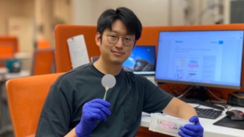
Postdoctoral fellow Seunguk Song applied a growth technique that overcame this shortcoming. Song and Deep Jariwala, associate professor in UPenn’s Department of Electrical and Systems Engineering (ESE) led the study, whose findings were published in Matter.
AI Business caught up with Jariwala to discuss his team’s research. (The interview was conducted by email.)
The inspiration comes from the known fact that silicon as a semiconductor material is reaching its physical limitations. This combined with the fact that we are doing more mobile and data heavy computing with all the smart devices means computing needs are fundamentally changing from arithmetic and multiplication heavy to data centric which also means greater use of memory and also low-power consumption overall.
2D materials are a broad class of crystals and compounds that are structurally, and in some cases chemically, stable at very small thickness under ambient conditions. This means you are able to produce films that are just one to three atoms in thickness that are electronically active and in many cases with electronic and optical properties far superlative to even 3D silicon.
However, the fair comparison to make is of a subclass of 2D materials, namely 2D semiconductors with silicon. A valid question to ask is, ‘How well can silicon perform if it is thinned down to one to three atoms in thickness?’ The answer is not well, in fact silicon may even cease to exist as crystalline silicon at those levels of thickness.
Therefore having 2D semiconductors that can vastly outperform silicon at small thicknesses is a great attribute of theirs. But then the question is why do we need small thicknesses? The short answer is to make even smaller transistors and circuits that consume even lower power per computation.
There are several ongoing and impending challenges to make microchips from 2D semiconductors. First, everything for semiconductor chipmaking has to be ultra-high quality and purity and devoid of contamination or defects to the extent possible. Second, the material needs to be made at least at the scale of 6-inch to 8-inch wafers, since all semiconductor production happens at ‘wafer-scale.’ We are not quite there yet in terms of 2D semiconductors.
In the past two to three years, substantial progress has been made to achieve wafer scale 2D semiconductors of reasonably high quality but several challenges remain in terms of making good and reliable transistor devices out of them. The other major challenge is integration of 2D semiconductors with other materials used in semiconductor manufacturing. All of these are vital issues.
We have been solving some of these challenges by growing wafer scale 2D semiconductors with high purity and high crystalline quality with minimal defects as one approach. But we are also trying to grow them at low-enough temperatures (lower than 400 to 500 centigrade) such that they can be integrated more easily with areas of semiconductor chip-manufacturing processes. The other problem we are trying to solve is to make better devices mainly by reducing the contact resistance and modulation of doping density. This also has been a persistent problem in the field which has seen some recent advances and we are also trying clever new ways to solve this problem.
This is a great question and a lot of people want to know the answer to this question just because of the crossroads semiconductor industry is currently at. My pragmatic answer to this is the following: I do not think we will be completely rid of silicon in the foreseeable future. Silicon will stay and remain a part of advanced microprocessors.
What will happen hopefully in less than a decade is that other materials such as 2D materials or germanium or III-V semiconductor materials may start getting paired with silicon for some devices and certain areas of the chips. What is also already happening and will accelerate moving forward is the growth of chips in the vertical direction. Think about this as more like a skyscraper instead of a strip mall, or a multi-story parking structure instead of a supermarket parking lot. The idea is to have more functionality added on top of silicon transistors which could be many things such as memory, sensing, communication or power delivery devices.
2D materials are also well suited to make a huge impact in this vertical ‘build-up’ popularly known as 3D heterogeneous integration in the chipmaking industry since one can think of them as sticky notes that can be peeled and pasted on any surface desired at high crystalline quality, something which is difficult to achieve for many other electronic materials.
In principle, it should have minimal impact on the manufacturing process because if the impact is too large, the cost benefit analysis becomes more steep and the argument for replacing or augmenting silicon falls apart. If that happens − I am pretty sure it should not − then such chips would occupy more niche markets such as defense, space, etc.
AI is all about computing at scale and with humongous amounts of data. This is where energy efficiency is truly important for AI hardware. While silicon hardware is currently improving in energy efficiency, the advances have been mostly at the architecture level. Pretty soon, people will run out of advances at the device level too. That is when we hit the fundamental limits of energy efficiency of computing as dictated by the physics of silicon based devices.
At that point, we are really only left with two or three options: change the material from silicon to something else like 2D materials which are the top contenders or change the physics of device operation, or both. So it is imperative that making chips from novel materials that are more energy efficient are beneficial for AI and big data computing in general. How much that truly translates into commercial impact and overall energy consumption from AI usage is unclear and remains to be seen.
This is connected to the previous answer. Deep-learning and neural networks can be classified among data heavy computing. Data heavy computing needs to become more efficient and this is what companies like Nvidia and others are trying to do by making innovations at the architecture level. But pretty soon they will run out of great ideas there and innovations will have to be made at the materials and physics level in the chips.
We hope to continue to make better transistors from 2D semiconductors and make them in ever-smaller dimensions and over larger and larger wafers. But we also hope to make 2D semiconductors practical for low-power embedded memory devices. This is something where we have recently made quite a bit of progress. Making low-power embedded memory with microprocessors will give birth to a new generation of AI hardware which could be orders of magnitude more efficient than what is currently available. We hope 2D materials and our memory materials and devices can make an impact in this space though there is a lot more work to be done.
You May Also Like
.jpg?width=700&auto=webp&quality=80&disable=upscale)
.jpg?width=700&auto=webp&quality=80&disable=upscale)
.jpg?width=700&auto=webp&quality=80&disable=upscale)
.jpg?width=300&auto=webp&quality=80&disable=upscale)
.jpg?width=300&auto=webp&quality=80&disable=upscale)
.jpg?width=300&auto=webp&quality=80&disable=upscale)
.jpg?width=300&auto=webp&quality=80&disable=upscale)
.jpg?width=300&auto=webp&quality=80&disable=upscale)